Electronica: Toshiba offers 130nm asic process for industrial applications
Read our full Electronica 2018 coverage »
Structured asics have a fixed array of logic in the underlying silicon, on to which custom metallisation is applied for each different application.
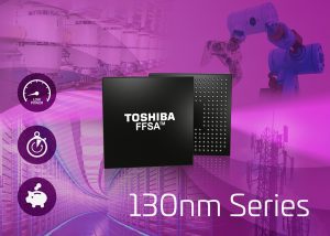
Toshiba brands this ‘FFSA‘ for ‘fit fast structured array’, and said: “The FFSA 130nm process is added to Toshiba’s current 28, 40, and 65nm process portfolio adding another option for industrial equipment. The 130nm node process offer different master slices for up to 664kb of RAM and around 912,000 gates per device.”
Structured asics are a half-way house on the route to full-custom asics where the silicon is custom too. Both types of asic are routes to SoCs.
“By limiting customisation to just the metal layer masks, it reduces development cost drastically,” said the firm. “As a result, samples and mass-produced devices can be delivered in a significantly shorter time than for conventional asics. Customers using the FFSA design methodology and library secure higher performance and lower power consumption than is possible withFPGAs.”
Devices designed on the platform will be manufactured by Toshiba subsidiary Japan Semiconductor.
Applications are expected in industrial equipment, communication equipment and OA equipment.